Report Overview
Global Polished Silicon Wafer Highlights
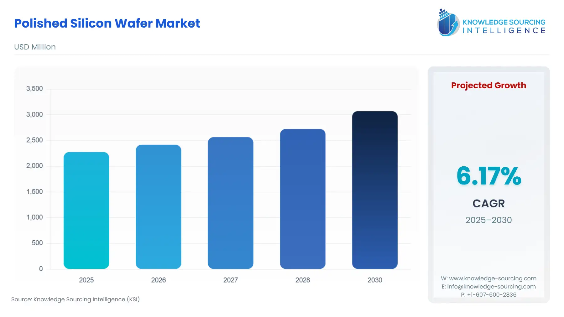
Polished Silicon Wafer Market Size:
The global polished silicon wafer market is projected to grow at a CAGR of 6.18% over the forecast period, increasing from US$2.276 billion in 2025 to US$3.071 billion by 2030.
The global polished silicon wafer market exhibits three main trends, including increases in diameters for denser chip layouts, enhanced efficiency, quality improvements to support future semiconductor technological developments, and the expanding requirement for SOI and SiC wafers because of peculiar applications.
Polished Silicon Wafer Market Overview & Scope:
The global polished silicon wafer market is segmented by:
- Type: By type, the global polished silicon wafer market has been segmented into N-type and P-type. N-type wafers contain a higher concentration of electrons, whereas P-type contains more holes in the absence of electrons. The two types use different electrical properties that guide them into specific semiconductor applications.
- Wafer Size: By wafer size, the market is segmented into small, medium, and large. For smaller applications that are older or less demanding, wafers with smaller diameters are normally used. When a balance is sought between the cost and the performance, medium-sized wafers are used. Advanced semiconductor manufacturing processes require very large-diameter wafers, such as those above 300mm, where more integrated circuits are produced per wafer, drastically influencing production yields and overall efficiency of manufacturing.
- Application: The polished silicon wafer industry applications are divided into consumer electronics, automotive and industrial usage telecommunications, and additional segments. Given the rapid growth trends, the Indian electronics industry expanded to reach a value of USD 155 billion in FY23. The production value of electronics rose from USD 48 billion in FY17 to USD 101 billion in FY23, mainly because mobile phones represent 43% of all facets of production. Additionally, mobile phone manufacturing in India accounts for 99% of total domestic production, while smartphone imports have diminished dramatically.
- Region: The North American polished silicon wafer market flourishes from three primary factors: the thriving domestic semiconductor industry enhanced by government initiatives such as the CHIPS and Science Act, increased demand for sophisticated electronics products, and the necessity of keeping supply chains local for resilience enhancement.
Top Trends Shaping the Global Polished Silicon Wafer Market:
1. Advancements in Semiconductor Technology
- Advancements in semiconductor technology are continuous processes. The quest for ever smaller and more powerful chips necessitates increasingly sophisticated manufacturing techniques. These complex modern devices require manufacturing bigger-diameter silicon wafers with higher overall quality specifications.
- The Semiconductor Industry Association (SIA)[1] reported semiconductor sales reached $57.8 billion in November 2024. The recorded total exceeds the November 2023 figure by 20.7%.
2. Government Initiatives
- Government initiatives are changing the landscape of the semiconductor industry. The United States executed the CHIPS and Science Act as a policy that distributes significant funding alongside incentives to advance local semiconductor manufacturing and research. The CHIPS and Science Act establishes policies to boost U.S. semiconductor manufacturing capability while protecting national technology leadership positions and strengthening supply chains.
Polished Silicon Wafer Market Growth Drivers vs. Challenges:
Opportunities:
- Expanding End-Use Markets: The rising adoption of smartphones, tablets, laptops, and IoT is continuously driving an advanced semiconductor usage requirement. Automobile companies are interested in electric cars, autonomous automobiles, and even advanced driver assistance systems, creating complex electronics that essentially depend on silicon wafers.
- Focus on Sustainability: The growing emphasis on sustainability in the semiconductor industry creates unique growth opportunities for polished silicon wafer manufacturers. Companies can enhance their brand image and gain a competitive advantage by focusing on environmental responsibility.
Challenges:
- High Production Costs: The main factor hindering market growth is the high production costs of manufacturing polished silicon wafers. Production is highly complex and capital intensive, involving crystal growth, cutting, polishing, and cleaning, and is associated with very high investments in equipment, infrastructure, and skilled labor.
- Supply Chain Disruptions: Supply chain disruption poses major challenges to the global polished silicon wafer market. The geopolitics of tension, natural calamities, and any event beyond expectation greatly disturb the raw materials and components necessary for making wafers.
Polished Silicon Wafer Market Regional Analysis:
- Asia-Pacific: Asia Pacific will have significant demand for the global polished silicon wafer owing to the strong presence of semiconductor manufacturing. The government of India, for instance, introduced the Semicon India Programme in December 2021 with an initial allocation of Rs.76,000 crore (US$9.2 billion) to fuel the growth of semiconductor and display manufacturing ecosystems in the country. In the interim Union Budget for 2024, India has raised the Semicon India Program's allocation to Rs. 6,903 crore (US$ 833.7 million).
Polished Silicon Wafer Market Competitive Landscape:
The market is fragmented, with many notable players, including Sigma Aldrich, WaferPro, and Sumco Corporation, among others:
- Product Launch: In June 2024, Onsemi announced plans to establish a state-of-the-art, vertically integrated silicon carbide (SiC) manufacturing facility in the Czech Republic.
Polished Silicon Wafer Market Scope:
| Report Metric | Details |
|---|---|
| Study Period | 2021 to 2031 |
| Historical Data | 2021 to 2024 |
| Base Year | 2025 |
| Forecast Period | 2026 – 2031 |
| Report Metric | Details |
| Polished Silicon Wafer Market Size in 2025 | US$2.276 billion |
| Polished Silicon Wafer Market Size in 2030 | US$3.071 billion |
| Growth Rate | CAGR of 6.18% |
| Study Period | 2020 to 2030 |
| Historical Data | 2020 to 2023 |
| Base Year | 2024 |
| Forecast Period | 2025 – 2030 |
| Forecast Unit (Value) | USD Billion |
| Segmentation |
|
| Geographical Segmentation | Americas, Europe, Middle East and Africa, Asia Pacific |
| List of Major Companies in the Polished Silicon Wafer Market |
|
| Customization Scope | Free report customization with purchase |
Polished Silicon Wafer Market is analyzed into the following segments:
By Type
- N-Type
- P-Type
- Small
- Medium
- Large
By Application
- Consumer Electronics
- Automotive
- Industrial
- Telecommunications
- Others
By Region
- Americas
- USA
- Europe, Middle East and Africa
- Germany
- Netherlands
- Others
- Asia Pacific
- China
- Japan
- Taiwan
- South Korea
- Others